
Heterogeneously integrated micro-ring with SnS2 for dual-functional optical modulation and photodetection
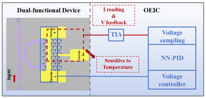
Fig. 1 | Schematic diagram of real-time feedback monitoring.
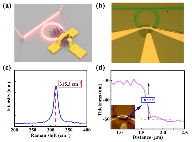
Fig. 2 | (a) Dual-function device architecture for optical modulation and photodetection based on SnS2 integrated with a microring resonator (MRR). Light is coupled in/out by two opposite grating couplers. (b) Microscope image of the device. (c) Raman spe
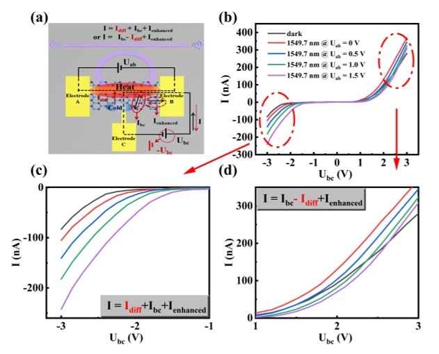
Fig. 3 | (a) Equivalent circuit diagram for synchronous optical modulation and detection. (b) I-Ubc characteristics at different modulation voltages Uab. (c) I-Ubc characteristics at Ubc < 0 V. (d) I-Ubc characteristics at Ubc > 0 V.
SHANNON, CLARE, IRELAND, July 24, 2026 /EINPresswire.com/ --
Announcing a new publication from Opto-Electronic Advances; DOI 10.29026/oea.2026.260042.
In advanced systems such as photonic integrated circuits (PICs) and optical neural networks, photodetectors and optical modulators serve as two fundamental functional modules. The former converts optical signals into electrical signals, a critical function for optical power monitoring and subsequent electronic processing. The latter loads electrical signals onto optical carriers, enabling dynamic control of optical transmission states. Their synergy forms the cornerstone of most optoelectronic computing and communication systems. Indeed, the core operating principles of both photodetectors and optical modulators center on the precise manipulation of light-matter interactions.
Traditional photonic computing and communication architectures rely on discrete, physically independent photodetectors and modulators. Specifically, optical power must be split by means of a bypass waveguide branch and directed into a dedicated photodetector. The resulting weak photocurrent, following amplification and conversion into a driving voltage, is then applied to another separate modulator. Such discrete interconnection links not only introduce substantial power consumption and transmission latency, but also increase chip manufacturing complexity, thereby constituting a fundamental bottleneck that restricts the development of high-density optical computing systems. Furthermore, the explosive growth of large language models (exemplified by ChatGPT) and various artificial intelligence applications has placed enormous demands on underlying hardware computing power. Compared with traditional electronic chips, photonic chips naturally offer advantages such as high bandwidth, low crosstalk, and low propagation loss. Nevertheless, a major challenge remains: how to efficiently integrate multiple optical functional modules on a single chip.
Two-dimensional (2D) materials address this challenge. Their atomic thickness, gate-tunable Fermi level, strong light-matter interaction, and ultrabroad spectral response enable co-integration of photodetection and modulation on the same waveguide platform. This work proposes and experimentally demonstrates a SnS2-silicon micro-ring heterogeneously integrated dual-function device. Without gate voltage, monolayer graphene, or any capacitive structure, the same microring platform simultaneously achieves a 23 dB modulation depth in the C-band and a photodetection responsivity of 0.38 A/W at −2 V.
Since the photon energy in the 1550 nm communication band is much lower than the intrinsic bandgap of SnS2, conventional interband absorption through band-to-band transitions cannot occur. However, by heterogeneously integrating SnS2 with a silicon microring resonator, this work leverages a pronounced bolometric effect, which induces a change in the device resistance and ultimately enables efficient photodetection in the 1550 nm infrared band. In addition, the designed gold heating electrode not only optimizes carrier transport and light absorption within the structure, but also enhances the generation efficiency of hot carriers. When a modulation signal is applied to the electrode, the average temperature rise, described by a thermal-resistance model, alters the refractive index of the microring resonator, thereby shifting the effective index of the waveguide mode and eventually the resonance wavelength. Benefiting from the synergy of this dual-channel multiplexed physical regulation mechanism, the proposed heterogeneously integrated device eliminates the external dependence on complex gate-voltage control, stringent monolayer material degradation, and capacitive structures, while paving a technological path toward the monolithic integration of detection and modulation functions on photonic chips.
Beyond improved performance metrics, this work provides a generic and flexible dual-function integration scheme. In traditional photonic circuit design, systems requiring both active signal modulation and real-time power monitoring typically tap a portion of the optical signal into a separate photodiode-a process that consumes chip area and introduces additional insertion loss. The proposed dual‑function device allows a single microring resonator to simultaneously act as both “controller” and “monitor”, yielding a more compact chip layout and a simplified photonic network architecture. The response time of the reported device is currently limited to the microsecond scale. Future research will therefore focus on two aspects: (i) further improving carrier transport speed through defect passivation, interface engineering, or the introduction of two-dimensional material systems with higher mobility; and (ii) exploring more efficient electro-thermal conversion structures, such as embedded thermal isolation trenches or heating materials with higher resistivity, to overcome the bottlenecks in modulation bandwidth and response speed. The integration concept and design strategy presented here point to a new direction for scalable, higher-density large-scale silicon photonic computing chips. Ultimately, a dual-port parallel feedback configuration combining real-time optical modulation and electrical readout will enable in-situ monitoring of the modulation state, achieving the high-level integration of dynamic tunability and self-diagnosis capability in photonic computing.
Keywords: two-dimensional materials, photodetectors, silicon microring resonator, silicon photonics
# # # # # #
The research team led by Professor Zhu Lianqing at Beijing Information Science and Technology University, supported by the Key Laboratory of the Ministry of Education and the National 111 Base, conducts research in collaboration with Tsinghua University and RMIT University in areas such as infrared detection technology, optoelectronic integrated devices, intelligent perception technology and systems, photonic computing chips, fiber optic sensing and systems, and optoelectronic and vision inspection systems. The team comprises more than 30 researchers, including those recognized as National Hundred, Thousand and Ten Thousand Talents Project recipients, National Young and Mid‑aged Expert with Outstanding Contributions, Beijing Scholar, National Model Teacher, and National Outstanding Science and Technology Worker, as well as over 290 doctoral and master’s students. The team has been recognized as a “Changjiang Scholars and Innovative Teams” program by the Ministry of Education, a Beijing Strategic Science and Technology Team, and a Beijing Outstanding Graduate Supervision Team. It has achieved a number of internationally leading research results, published over 500 academic papers, been granted more than 160 invention patents, and published 4 monographs. The team has received the Second Prize of the National Science and Technology Progress Award, the First Prize of Technological Invention from the Ministry of Education, and more than 10 provincial/ministerial‑level awards. These research achievements have been widely applied in aerospace, advanced manufacturing, national defense, and military fields.
# # # # # #
Opto-Electronic Advances (OEA) is a high-impact, open access, peer reviewed SCI journal with an impact factor of 22.4 (Journal Citation Reports 2024). OEA has been indexed in SCI, EI, DOAJ, Scopus, CA and ICI databases, and expanded its Editorial Board to 41 members from 17 countries.
# # # # # #
More information: http://www.oejournal.org/oea
Editorial Board: http://www.oejournal.org/oea/editorialboard/list
All issues available in the online archive (http://www.oejournal.org/oea/archive).
Submissions to OEA may be made using ScholarOne (https://mc03.manuscriptcentral.com/oea).
ISSN: 2096-4579
CN: 51-1781/TN
Contact Us: oea@ioe.ac.cn
Twitter: @OptoElectronAdv (https://twitter.com/OptoElectronAdv?lang=en)
WeChat: OE_Journal
# # # # # #
Du JY, Lu LD, Zhang X et al. Heterogeneously integrated micro-ring with SnS2 for dual-functional optical modulation and photodetection. Opto-Electron Adv, 260042 (2026). DOI: 10.29026/oea.2026.260042
Opto-Electronic Advances Editorial Office
Opto-Electronic Advances
+86 591 2286 1222
email us here
Legal Disclaimer:
EIN Presswire provides this news content "as is" without warranty of any kind. We do not accept any responsibility or liability for the accuracy, content, images, videos, licenses, completeness, legality, or reliability of the information contained in this article. If you have any complaints or copyright issues related to this article, kindly contact the author above.
