Strain engineering in van der Waals materials for flexible electronics and optoelectronics
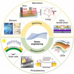
GA, UNITED STATES, December 12, 2025 /EINPresswire.com/ -- Strain engineering precisely tunes van der Waals materials' electronic and optical properties for flexible electronics. This review covers uniaxial, biaxial, and localized strain methods, analyzing their effects on band structure, carrier mobility, and phase transitions. Applications include high-performance sensors, transistors, memristors, photodetectors, and LEDs. Future challenges involve scalable material growth, efficient strain transfer, and integration toward intelligent wearable systems.
Van der Waals (vdW) materials exhibit exceptional mechanical flexibility and electronic properties, making them promising candidates for next-generation flexible electronics. Notably, their atomic thinness allows reversible elastic deformation that far exceeds conventional semiconductors. Strain engineering exploits this compliance to tune physical properties through controlled lattice distortion.
In a recent review published in Wearable Electronics, a team of researchers from China and South Korea presents an analysis that unifies these interrelated elements, including strain application strategies, modulation of physical properties, and device-level implementation, into a cohesive framework for the design and optimization of high-performance flexible vdW electronic and optoelectronic systems.
In particular, three primary mechanisms exist for applying strain. Uniaxial deformation stretches the lattice along one axis, breaking crystalline symmetry and creating anisotropic electronic behavior. Biaxial strain induces uniform in-plane expansion or compression, preserving symmetry while modulating band structure isotropically. Local strain generates spatially confined distortions through substrate patterning, producing property gradients. Efficient transfer requires strong interfacial coupling, often enhanced via encapsulation.
The strain's fundamental impact originates at the atomic level. Mechanical deformation alters bond lengths and angles, modifying orbital overlap and hybridization. This reshapes the electronic band structure: bandgap energies shift, band edges realign, and curvature changes affect carrier effective mass. Tensile strain typically reduces bandgap and decreases effective mass, enhancing mobility.
Sufficient strain can lower activation barriers for structural phase transitions, enabling switching between semiconducting and metallic states. Symmetry breaking activates piezoelectric effects in non-centrosymmetric lattices, where mechanical deformation generates internal electric fields that further modulate band alignment.
Taken together, these physical changes translate directly to device functionality. In sensors, strain-modulated band edges alter carrier concentration and barrier heights, enhancing sensitivity. For logic elements, reduced effective mass increases transistor mobility, while strain-assisted phase transitions enable low-power memristive switching for in-memory computing. In optoelectronics, bandgap tuning controls spectral response and emission wavelengths. The piezoelectric effect couples mechanical strain to electrical and optical responses, enabling additional functionality.
The authors note the existing key challenges. Scalable synthesis of uniform, high-quality materials with precise thickness control is difficult. Transferring films to flexible substrates without damage requires improved techniques. Most critically, weak interfacial bonding limits strain transfer efficiency. Solutions include high-surface-energy intermediate layers and integrating strain during synthesis.
The team believe that future advances would depend on synergistic development of synthesis, strain application, and device architectures. Combining intrinsic multimodal sensing capabilities with strain engineering and memory technologies will enable adaptive systems integrating sensing, memory, and computation. These multimodal platforms can then simultaneously detect mechanical, chemical, and optical stimuli, mimicking biological sensory systems.
“Such integration will enable intelligent human-machine interfaces and continuous health monitoring through bioinspired electronic skin,” says corresponding author Zhongming Wei. “Realizing this potential requires manufacturable processes that maintain structural integrity and performance uniformity across large areas.”
References
DOI
10.1016/j.wees.2025.10.001
Original Source URL
https://doi.org/10.1016/j.wees.2025.10.001
Funding information
This work was financially supported by the National Key Research and Development Program of China (Grant No. 2024YFA1409700), the National Natural Science Foundation of China (Grant No. 62125404, U24A20285, 62375256, 62174155, 62334007, 12334005, 12304540), Beijing Natural Science Foundation (Z220005), Science Foundation of the Chinese Academy of Sciences (Grant No. JCPYJJ-22), and CAS Project for Young Scientists in Basic Research (No. YSBR-056).
Lucy Wang
BioDesign Research
email us here
Legal Disclaimer:
EIN Presswire provides this news content "as is" without warranty of any kind. We do not accept any responsibility or liability for the accuracy, content, images, videos, licenses, completeness, legality, or reliability of the information contained in this article. If you have any complaints or copyright issues related to this article, kindly contact the author above.

