3D-printed facet-attached microlenses (FaML) could overcome photonic packaging challenges

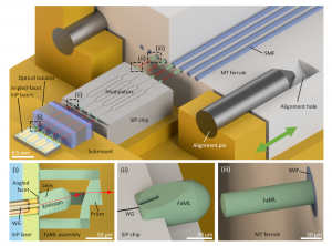
See Insets (i), (ii), and (iii) that expand and match the mode fields of the different components and enable low-loss coupling with relaxed alignment tolerances.
Photonic integrated circuits (PIC) are on the verge of significant disruption through the unlocking of novel applications. This success largely relies on advanced wafer-level miniaturized photonic device fabrication, combining outstanding functionality and robustness with unprecedented performance and scalability.
However, while cost-efficient mass production of PIC has become widely available through dedicated foundry services, scalable photonic packaging and system assembly still represent a significant challenge and an obstacle towards accelerated commercial uptake.
Specifically, package-level optical chip-to-chip and fiber-to-chip connections often rely on so-called butt coupling, where device facets are brought close or in direct physical contact. This approach usually requires high-precision active alignment with sub-micrometer accuracy, thus complicating assembly processes. Moreover, matching the mode fields can be challenging, particularly when connecting waveguides with vastly different refractive-index contrasts.
In a new paper published in 'Light: Applied Manufacturing', a team of scientists led by Dr Yilin Xu and Professor Christian Koos from Karlsruhe Institute of Technology (KIT) have demonstrated that 3D-printed facet-attached microlenses (FaML) can overcome the scalability challenges of PIC-based solutions.
FaML can be printed with high precision to the facets of optical components using multi-photon lithography, thereby offering the possibility to shape the emitted beams by freely designed refractive or reflective surfaces. Specifically, the beams can be collimated to a comparatively large diameter independent of the device-specific mode fields. This approach relaxes axial and lateral alignment tolerances. Their findings mean that costly active alignment becomes obsolete and can be replaced by passive assembly techniques based on machine vision or simple mechanical stops. Moreover, the FaML concept allows inserting discrete optical elements, such as optical isolators or polarization beam splitters, into the free-space beam paths between PIC facets.
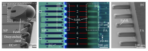
Building upon their previous work, the researchers showed the scheme's viability and versatility in a series of selected demonstrations of high technical relevance. In the first set of experiments, they coupled fiber arrays to arrays of edge-coupled silicon photonic (SiP) chips, reaching insertion losses of 1.4 dB per interface with a translational lateral 1 dB alignment tolerance of ± 6 μm. This is the lowest loss demonstrated for an edge-emitting SiP waveguide interface with micron-scale alignment tolerances. The researchers further demonstrated that their scheme's outstanding alignment tolerance allows contactless pluggable fiber-chip interfaces using conventional injection-molded parts.
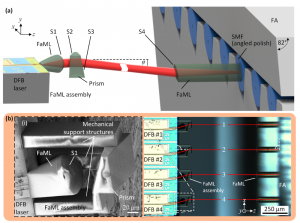
In a second set of experiments, they demonstrated free-space transmission over distances in the mm range, using standard machine-vision techniques for alignment. A third set of experiments is finally dedicated to interfaces between InP lasers and SMF arrays. In these experiments, the researchers demonstrated the coupling of planar devices through non-planar beam paths comprising only tilted optical surfaces, thus offering ultra-low back-reflection.
Based on their exemplary demonstrations of the outstanding versatility of the FaML approach, the researchers believe that their concept opens an attractive path towards advanced photonic system assembly that may overcome most of the current challenges. Opening a path towards scalable and flexible photonic packaging concepts that complement wafer-level mass fabrication of the underlying PIC, the FaML concept addresses one of the most stringent challenges of integrated optics today.
###
References
About Light: Advanced Manufacturing (LAM):
Light: Advanced Manufacturing (LAM) is a new, highly selective, open-access, and free-of-charge international sister journal of the Nature Journal Light: Science & Applications. The journal aims to publish innovative research in all modern areas of preferred light-based manufacturing, including fundamental and applied research and industrial innovations.
Funding:
This research received funding from the Deutsche Forschungsgemeinschaft (DFG, German Research Foundation) under Germany's Excellence Strategy via the Excellence Cluster 3D Matter Made to Order (3DMM2O) and the Collaborative Research Center WavePhenomena, by the Bundesministerium für Bildung und Forschung (BMBF) via the projects PRIMA, DiFeMiS, which is part of the programme "Forschungslabore Mikroelektronik Deutschland (ForLab), and Open6GHub, by the European Research Council (ERC Consolidator Grant TeraSHAPE), by the H2020 Photonic Packaging Pilot Line PIXAPP, by the Alfried Krupp von Bohlen und Halbach Foundation, and by the Karlsruhe School of Optics and Photonics (KSOP).
Authors:
Yilin Xu, Pascal Maier, Mareike Trappen, Philipp-Immanuel Dietrich, Matthias Blaicher, Rokas Jutas, Achim Weber, Torben Kind, Colin Dankwart, Jens Stephan, Andreas Steffan, Amin Abbasi, Padraic Morrissey, Kamil Gradkowski, Brian Kelly, Peter O’Brien, Wolfgang Freude and Christian Koos
DOI: 10.37188/lam.2023.003
Paper Title: 3D-printed facet-attached microlenses for advanced photonic system assembly
Original Source URL: https://light-am.com/article/doi/10.37188/lam.2023.003
Article Publication Date: 17 April 2023
Wendy Chen
TranSpread
email us here
Legal Disclaimer:
EIN Presswire provides this news content "as is" without warranty of any kind. We do not accept any responsibility or liability for the accuracy, content, images, videos, licenses, completeness, legality, or reliability of the information contained in this article. If you have any complaints or copyright issues related to this article, kindly contact the author above.


